Optical Pattern Recognition and Image Processing
Abstract
Recognition and processing of optical patterns and images by electronic computers are computationally demanding and require conversion of large quantities of optical information into electronic data. Therefore, the inherent parallelism of photonic systems has long been considered to be the route toward faster, less complex, and more energy efficient real-time pattern recognition and image processing systems. Optical Fourier techniques and spatial light modulators have been widely employed in image processing techniques intended for medical imaging. However, the ultimate potential of photonic systems is revealed when optical logic computations come into play. Optical pattern recognitions have been realized with different types of optical correlators based on photorefractive polymers, semiconductor optical amplifiers, delay lines, and phase shifter designs. Photorefraction, phase conjugation, second-harmonic generation, vapor atomic transitions with four-wave mixing, spatial dispersers, and reservoir computing systems have served as the basis of reliable all-optical image processors.
Three major factors are essential for developing deep learning approaches and technologies: data, algorithms, and computational capacity. Data processing and algorithm implementation require the technical support of the chips in the application terminal, with current deep learning chip technologies primarily including graphics processing units, field-programmable gate arrays, and application-specific integrated circuits.
Optical neural networks and photonic circuits provide a novel dedicated neural network accelerator to exploit the parametric changes of optics for computing. Optical computing systems can be massively parallel or combined with small form factor devices. Photonics offers the advantages of high speed, high bandwidth, and low power consumption compared with electronics. Photonic solutions can significantly reduce the power consumption of logic and data operations. It is well known that an ordinary lens can perform a Fourier transform without consuming any energy and that certain matrix operations can be performed with no energy consumption. Many inherent optical nonlinearities can be directly used to implement nonlinear operations with photons. Once a neural network has been trained, the architecture can be passive, and computations on the optical signal can be performed without additional energy input. Optical interconnects can allow hybrid optoelectronic deep neural networks, where low-energy, highly parallel integration techniques can be used as part of an analog optical processor.

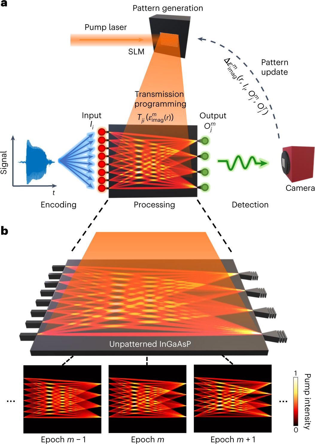
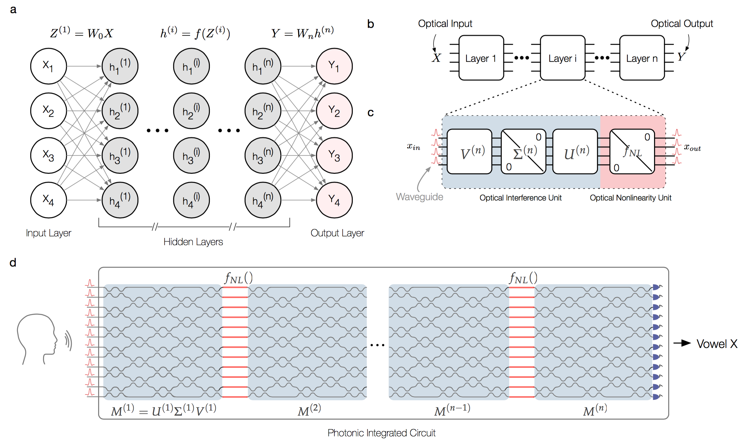
More recently, the rapid development of silicon optical integration technology has provided technical support for research into photonic integrated neural network chips. Photonic integrated neural networks are used to perform matrix multiplication and addition calculations (MACs) in neural networks, using photon integration technology to run deep learning algorithms and implement machine learning-related applications. Conceptual exploratory research work has already been conducted on the use of photonic integrated neural network chips to implement neural network operations, and there is the hope of using photonic integrated neural network chips to accomplish tasks such as image classification and object detection for applications in servers, autonomous driving, and other scenarios. Integrated photonics, because of its intrinsic high speed, large bandwidth and unlimited parallelism, is critical in the drive to ease the increasing data traffic. Its technological enabler is high-precision lithography, which allows for the fabrication of high-resolution photonic structures. Here, in complete contrast to the state of the art, where photonic functions are predefined by lithographically modulating the real index, we report a lithography-free paradigm for an integrated photonic processor, targeting dynamic control of spatial-temporal modulations of the imaginary index on an active semiconductor platform, without the need for lithography. We demonstrate an imaginary-index-driven methodology to tailor optical-gain distributions to rationally execute prescribed optical responses and configure desired photonic functionality to route and switch optical signals. Leveraging its real-time reconfigurability, we realize photonic neural networks with extraordinary flexibility, performing in situ training of vowel recognition with high accuracy.
Photonic neural networks offer a promising alternative to microelectronic and hybrid optoelectronic implementations, where classical neural networks rely heavily on fixed matrix multiplication. However, the need for phase stabilization and many neurons with large optical components, such as fibers and lenses, has been a major obstacle to achieving this conversion. Integrated photonics solves this problem by providing a scalable solution. Photon particles are too large to be integrated at the same high level as electrons. In addition, present optical neural network solutions inevitably rely on electronics. Submicron-scale etching techniques are still not available, and height differences and spacing between optics and electronics and process incompatibilities make optoelectronic integration challenging. Furthermore, nonlinear limitations and photonics integration constraints make it impossible to scale chips such as electronic neuromorphic computing chips, which are mere arrays.
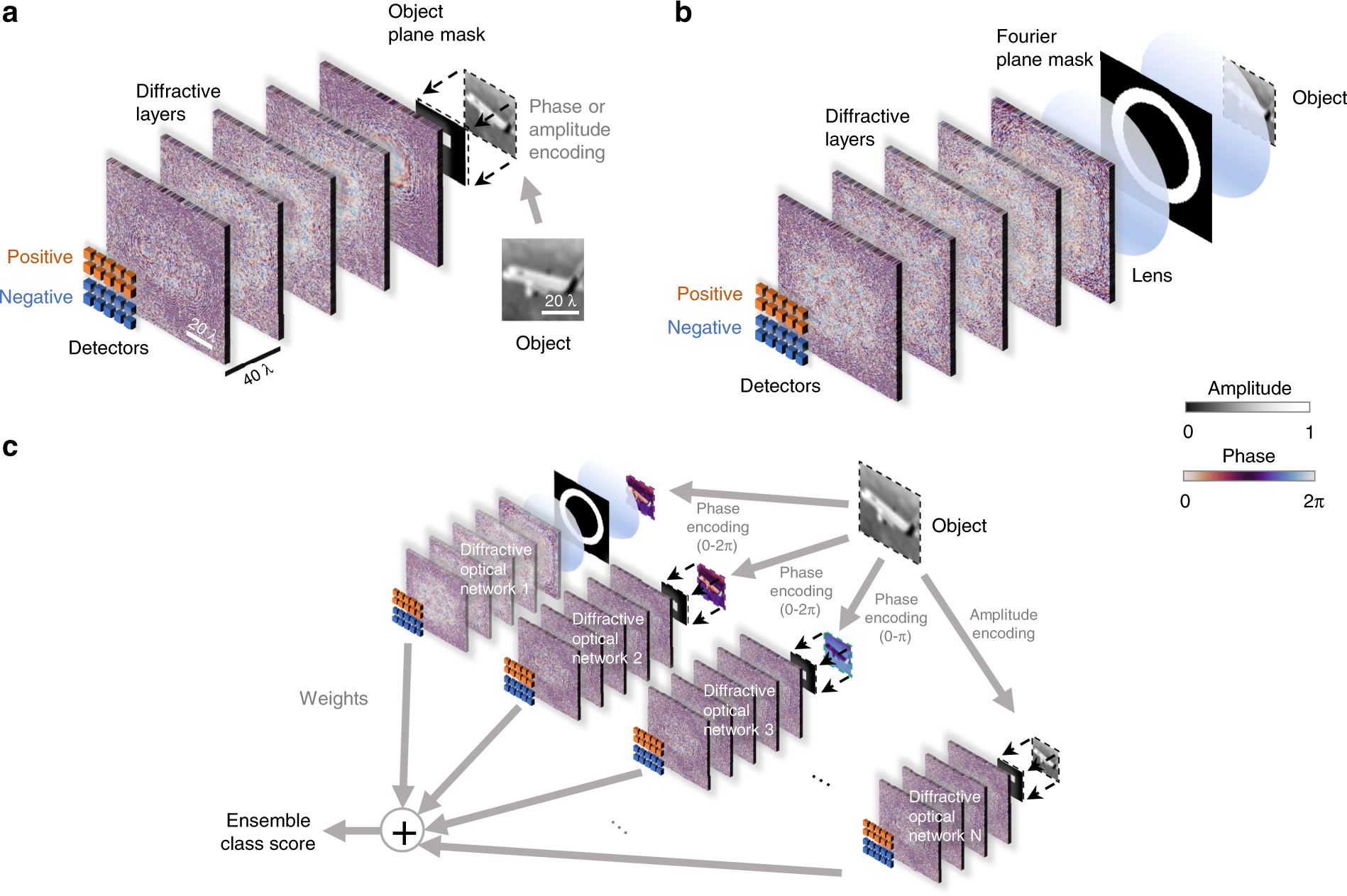
Optical neural networks have been studied in Fourier optics for decades, and the forward physical structure of multilayer coherent neural networks is thought to be promising. Deep diffraction neural networks (D2NNs) have been proposed for various classification tasks and high-dimensional information via optical processing, with millions of neurons and hundreds of billions of connections. D2NNs also enable image saliency detection in Fourier space. Diffraction is a prevalent physical phenomenon of incoherent light propagation. Any point in the plane perpendicular to the direction of propagation can be interpreted as a coherent superposition of complex amplitudes of integral points in the reference plane with a certain diffraction distance. The superposition of diffraction meets the basic requirements of deep complex neural networks. Therefore, as an optical mechanism, coherent diffraction can provide an alternative method to fully connect multi-valued neurons. The training input of the underlying D2NN model is operated via spatial features. The input domain is filtered in the object or Fourier space by introducing a series of ordered passive filters prior to the diffraction network. This allows for the parallel processing of optical information.
Machine learning has evolved to the point where there is an urgent need for computationally small, low-latency datasets to reduce the computational effort associated with computational power limits and large datasets. When inputting data, nonlinear optical dynamics enables linear learning algorithms to learn nonlinear functions or determine boundaries to classify the data into correct classes. The Lambda kernel is capable of nonlinearly casting data that have been modulated onto the spectrum of femtosecond pulses into a space where data that are non-dividable in linear terms are converted to be linearly divisible in the new space. In terms of functionality, there are similarities between the Lambda kernel and the concept of “kernel projection” in the machine learning literature. Using this approach, the spectrum of the data is mapped onto femtosecond light pulses and projected into an implicit high-dimensional space using nonlinear optical dynamics, thereby improving the accuracy and reducing the latency in the data classification by several orders of magnitude. The nonlinear dynamics are introduced into the data before processing the output data with an optical classifier.

Printing with Light
Here, neural lithography is introduced to address the ‘design-to-manufacturing’ gap in computational optics. Computational optics with large design degrees of freedom enable advanced functionalities and performance beyond traditional optics. However, the existing design approaches often overlook the numerical modeling of the manufacturing process, which can result in significant performance deviation between the design and the fabricated optics. To bridge this gap, we, for the first time, propose a fully differentiable design framework that integrates a pre-trained photolithography simulator into the model-based optical design loop. Photonic integration renders ultrafast artificial neural networks possible, and photonic neuromorphic computing results in challenges different from those of electronic computing. Algorithms running on such hardware can meet the growing demand for deep learning and artificial intelligence in areas such as medical diagnostics, telecommunications, and high-performance and scientific computing. All calculations will be performed at the speed of light, which is much faster than the analog speed of digital computers, therefore processing exponentially more data. For real-time observations, time-stretch processors are ideal output devices. Even though photonic neuromorphic computing is still in its infancy, this research area has great potential to expand the frontiers of deep learning and information processing.
Photonic neural networks computing is a system comprising active and passive devices, light sources, and transistors. However, no fabrication platform is yet capable of implementing all of these functions upon a single mold based on current fabrication levels. Present optical neural network solutions still exclusively rely on electronics. Optoelectronic integration processes remain challenging because submicron-scale etching techniques are still unavailable, and issues such as height disparities, spacing restrictions, and process incompatibilities are still prevalent. Currently, on-chip light sources use a concatenation of III–V families of materials or a direct epitaxy of quantum dot lasers on silicon. However, the complexity of the preparation process and associated reliability cannot meet the commercial mass production standards. Several approaches for integrating photonic systems and CMOS sensors for ultimately achieving a successful on-chip photonic neural network design are presently being explored.

Photolithographic Patterning
This neural lithography technique could help scientists and engineers create more accurate and efficient optical devices for applications like mobile cameras, augmented reality, medical imaging, entertainment, and telecommunications. And because the pipeline of learning the digital simulator utilizes real-world data, it can be applied to a wide range of photolithography systems.
Difficulties associated with on-chip optical delays are also a challenge being evaluated currently. Nonlinear operations are an indispensable and important part of neuromorphic computing. Moreover, non-volatile photonic storage and weighting as well as low power consumption are necessary to ensure neurosynaptic function. Although photonic nonlinear neural operations have been demonstrated in materials such as PCM, a large gap still remains regarding electronic nonlinear neuromorphic operations. Accordingly, there is still room for development in energy efficiency and fast switching of new accumulable materials. In addition, training is one of the key steps for the vast majority of neural network algorithms, which to date still requires implementation.
The new technology overcomes the conventional limits that are known from standard optical mask aligners. Standard mask aligners generally run into the issue that the resolution is limited to about 3.0 μm for proximity configuration. This means the photomask is placed in the vicinity of the wafer forming a 20-100 μm separation gap during exposure. This resolution simply does not meet the requirements for Patterned sapphire substrates (PSS) and nano-patterned sapphire substrates (nPSS). However, the technology, which is built on standard, cost and throughput optimized mask aligner technology, permits printing of such small feature sizes. Its unique property is the down to 150 nm printing resolution for regular patterns in a single exposure step. Nonetheless, a mask-substrate separation gap of several tens of microns is kept while the image depth can be extended to cover the multiple micron thick resist without resolution deterioration. This very high aerial image aspect ratio allows printing of the same high-resolution patterns onto large and highly warped surfaces, such as LED wafers.

The demand for increased data processing volumes and operation speeds is constantly growing, and it is urgent to circumvent the structural von Neumann bottleneck and design new structures to accommodate efficient neural network training and testing. Optical processors, with their advantages of high speeds and low power consumption, have been gaining attention as a result of the rapid development of hardware dedicated to the inference and training of optical neural networks. Optical neural networks have shown great promise in terms of low-energy consumption and high-speed parallel computing, and the development trend of optical neuromorphic computing appears to be unstoppable. According to research findings, photonic neuromorphic computing is currently in its preliminary developmental stage, and various optimization solutions have emerged, even though photonic neural networks still have many challenges to overcome.
